Assembled Circuit Boards Tested
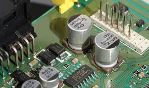
Assembled circuit boards undergo multiple tests to ensure they function as intended. These tests can be categorized as basic, in-circuit, and functional. Basic testing is designed to identify issues before they become serious problems, in-circuit testing examines each component as it’s soldered into place and functional testing checks the entire board at different levels of functionality. Each of these tests has specific procedures that must be followed to ensure accurate and reliable results.
Basic testing typically consists of visual inspection and automated optical inspection. In addition to these inspections, a PCB assembly may also undergo electrical and mechanical testing to detect any issues that could affect its performance. In-circuit test (ICT) examines each individual component in the assembled circuit board to make sure it is in the correct location and that its value matches the original design. It can also be used to detect open circuits, shorts, and wrong parts.
In-circuit testing involves using software and fixtures to interface several instruments with the PCB assembly under test. This allows production line workers to perform this type of testing automatically. Engineers develop the firmware for each testing requirement using high-level computer languages. These programs control the test system, determine the points to be tested, and set the values for the pass/fail criteria. These programs are then loaded into a fixture, which is a mechanical device that holds the circuit board under test and makes contact with the test points.
How Are Assembled Circuit Boards Tested?
For example, a fixture may use a standard “bed-of-nails” tester, which has a number of probes that can be moved around the circuit board to contact each of the test points. Other systems, such as flying probes, are powered by software and do not require a physical fixture to make contact with the assembled circuit board. These systems are more affordable than ICT fixtures, but they can be difficult to program for each new board design and may not offer as much physical access to the test points as ICT test systems do.
X-ray imaging can be useful for examining the internal structure of an assembled circuit board, including components and solder joints. It can also provide a clear view of any flaws or anomalies in the PCB’s manufacturing process, such as holes that are too close together or traces that are too close to other traces. This type of defect can often be detected and corrected before the board is sent for final assembly, preventing expensive rework and scrap.
Although not a type of PCB testing, Design for Testing (DFT) is an important tool that can help manufacturers avoid defects and reduce costly rework costs. This approach involves designing the circuit board to make it easier to test its quality and functionality. This can involve creating test points that are easier to access with automated test equipment and providing adequate spacing between these test points and other design objects like outlines or pads.